
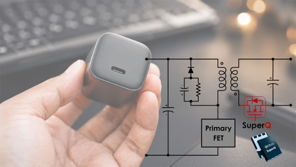
Quasi-resonant (QR) flyback converters have become the topology of choice for power supplies in the 45W to 120W range, powering everything from USB-C chargers to embedded industrial power supplies. Their combination of simplicity, cost-effectiveness, and high efficiency has made them a staple in modern power conversion.
Traditionally, improving the efficiency of quasi-resonant (QR) flyback converters has centered on the primary-side switch. But as primary-side losses continue to shrink, the synchronous rectifier (SR) on the secondary side has become an increasingly important contributor to overall converter performance.
A recently published article in Electronic Design examines why the synchronous rectifier should be viewed as a system-level design element rather than simply a low-loss switch. The findings demonstrate that the dynamic characteristics of the SR MOSFET can influence the behavior of the entire converter, including the primary-side switch.
The Synchronous Rectifier Is More Than a Conduction Device
In a conventional design process, engineers often select the SR MOSFET by minimizing conduction losses. Lower RDS(on) generally translates into higher efficiency during the secondary conduction interval.
However, QR flyback converters behave differently than many other topologies.
Because switching events are governed by a resonant network formed by the transformer magnetizing inductance and parasitic capacitances, the synchronous rectifier becomes an active participant in the converter’s resonant operation. Device characteristics such as output capacitance (COSS) and switching charge (QSW) influence not only secondary-side conduction but also transformer reset behavior, resonant timing, voltage ringing, and primary-side switching losses.
This system-level interaction means that selecting an SR MOSFET solely on RDS(on) can overlook opportunities for meaningful efficiency and thermal improvements.
Looking Beyond Traditional Silicon Tradeoffs
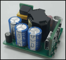
Figure 1: 65W USB-C QR Flyback Converter (PCBA = 39 x 34 x 17mm)
Traditional silicon MOSFET design has always involved balancing competing parameters. Lower on-resistance often comes at the expense of higher capacitance or increased switching losses, forcing designers to compromise depending on the application.
The Electronic Design article explores how iDEAL Semiconductor’s patented SuperQ® architecture changes that equation.
Unlike conventional superjunction devices, SuperQ uses an asymmetrical charge-balanced structure that increases conduction-area utilization while maintaining high-voltage blocking capability. The result is a device that simultaneously delivers lower conduction losses, lower output capacitance, faster switching behavior, and improved resonant performance. Rather than improving only one aspect of device performance, the architecture enables improvements that propagate throughout the converter.
Putting the Theory to the Test
To evaluate these system-level effects, a 65 W USB-C QR flyback converter operating from a universal AC input (90–264 VAC) with a 20 V, 3.25 A output, shown in Figure 1, was tested.
The only variable changed during testing was the synchronous rectifier MOSFET. Control circuitry, PCB layout, transformer, and external components remained identical, allowing the measured performance differences to be attributed directly to the SR device.
The results demonstrated that optimizing the synchronous rectifier can improve overall converter behavior, not just secondary-side efficiency.
Among the measured improvements:
- Up to 0.5% higher overall efficiency
- Approximately 0.3 W lower total converter power loss
- Nearly 25% faster primary-side drain-voltage transitions
- More than 20°C lower primary-side operating temperature under high-line conditions
Improving the Primary Side from the Secondary Side
One of the most interesting findings from the evaluation is that improvements made on the secondary side translated directly into lower switching losses on the primary side.
Because the synchronous rectifier contributes to the converter’s resonant tank, reducing stored charge and output capacitance changes how energy circulates during each switching cycle.
With less reflected capacitance in the resonant network, the primary switch experiences:
- Faster drain-voltage transitions during turn-off
- Reduced overlap between voltage and current
- Lower switching losses
- Lower drain voltage at turn-on
- Reduced EOSS-related losses
The measurements in Figure 2 show that the primary switch rise time decreased from approximately 72ns to 55ns, a reduction of nearly 25%. This demonstrates that the synchronous rectifier is not simply improving its own efficiency; it is actively improving the operating conditions of the primary switch.
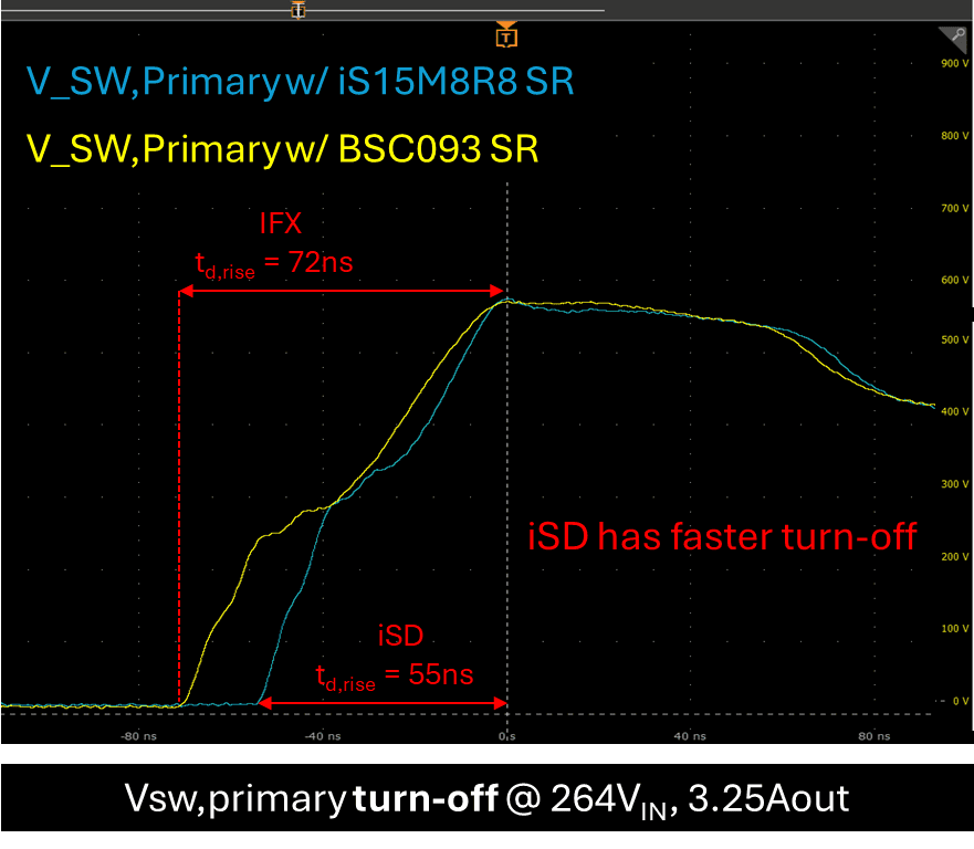
Figure 2: Primary switch drain-voltage turn-off transition at VIN = 264 VAC, VOUT = 20 V, IOUT = 3.25 A comparing conventional superjunction and SuperQ SR devices.
Thermal Benefits
Efficiency improvements are valuable, but thermal performance is often what determines whether a design succeeds in the real world.
Thermal imaging of the evaluation platform revealed that while secondary temperatures remained comparable across devices, the primary-side power stage experienced dramatically lower operating temperatures when using the iS15M8R8S1C SuperQ MOSFET as the synchronous rectifier.
At high input voltage, the primary module temperature dropped by more than 20°C compared with a conventional silicon solution, as shown in Figure 2.
Lower operating temperatures can translate into numerous practical benefits, including improved long-term reliability, increased power density, smaller cooling requirements, greater design margin, and improved robustness.
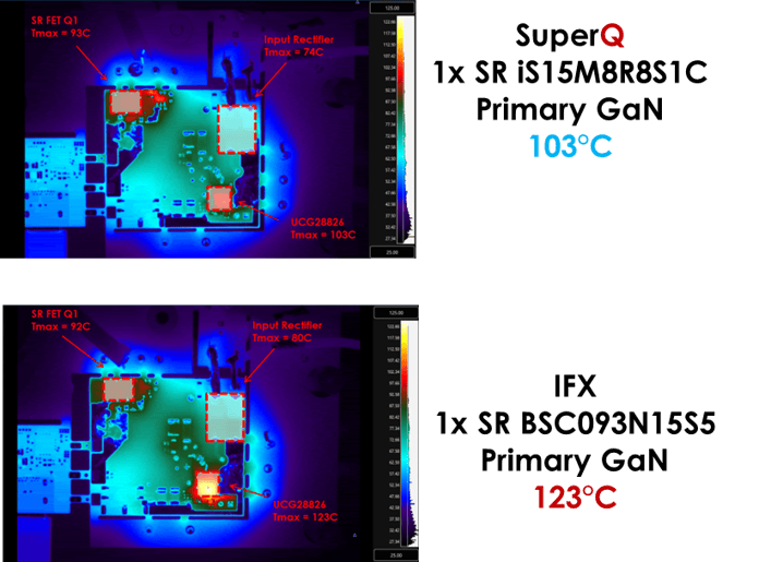
Figure 3: Thermal comparison of converter with SuperQ in the QR vs. Conventional Silicon MOSFET in the QR at 264VAC
Read the Complete Technical Article
The synchronous rectifier has evolved from a passive conduction device into an active contributor to resonant switching behavior, converter efficiency, thermal performance, and overall system optimization.
For engineers designing next-generation USB-C adapters, embedded power supplies, and other QR flyback applications, understanding these interactions can unlock measurable improvements without changing converter topology or control architecture.
The full article published in Electronic Design explores the underlying device physics, measurement methodology, oscilloscope waveforms, thermal images, and detailed experimental results behind these findings.
Read the full article on Electronic Design: Rethinking the Synchronous Rectifier in QR Flyback Converters | Electronic Design