Silicon Power Devices: A New Chapter in Silicon Innovation
Data centers already account for more than 2% of global electricity consumption, and the IEA forecasts this will exceed 1 petawatt annually by 2026. In the U.S. alone, demand is expected to reach 1 petawatt by 2030 — driven largely by AI, hyperscale infrastructure, and high-performance computing (HPC).
As these workloads scale, efficiency is everything. Programs like 80 PLUS, ENERGY STAR, and custom OEM standards are enforcing tighter efficiency margins at every power conversion stage.
Meeting these requirements is pushing the limits of conventional silicon power devices and creating demand for new architectures that deliver lower losses, higher efficiency, and improved ruggedness.
For decades, silicon has been the preferred material for power semiconductors, thanks to its abundance, cost-effectiveness, mature manufacturing ecosystem, and proven reliability. It remains the dominant substrate in electronics, with estimates showing that over 90-95% of all semiconductor devices continue to use silicon.
One of the most important breakthroughs in silicon was the introduction of the Superjunction MOSFET, which dramatically improved performance compared to earlier planar designs. However, Superjunction devices are reaching practical limits. Their design constrains conduction area, and further on-state resistance (RDS(on)) reductions often require more complex and costly processing, which can limit their scalability for high-performance applications.
To meet the growing demands of today’s power systems – without leaving behind the silicon infrastructure that the industry depends on – a new architecture was needed.
In 2025, that breakthrough arrived with SuperQ®
SuperQ is a revolutionary asymmetrical reduced surface field (RESURF) structure that achieves near-ideal charge balance, allowing for thinner epitaxy and significantly improved performance figures of merit.
Compared to Superjunction devices, SuperQ increases conduction area by up to 2x, achieves dramatically lower on-resistance and switching losses, and reduces inverter losses by up to 46% - all while maintaining the cost, availability, and reliability advantages that have made silicon the industry standard.

Contents
History of silicon power semiconductors (1950 to 2024)
The first silicon-based transistors were developed in the mid-20th century, revolutionizing electronics. Early silicon transistors were primarily used for signal amplification, but as technology progressed, their ability to handle higher power levels increased.
Silicon's abundance, relative low cost, and well-established manufacturing processes have made it the dominant material in power electronics to this day.
Key milestones in the development of silicon power devices include:
1950s & 1960s
Development of the first silicon transistors and diodes. Prior to this, power rectification was undertaken by vacuum tubes and selenium rectifiers, followed by diodes based on germanium.
1970s
Introduction of power MOSFETs (Metal-Oxide-Semiconductor Field-Effect Transistors), which offered improved switching speed and efficiency compared to bipolar transistors.
1980s & 1990s
In 1982, the first experimental demonstration of the discrete vertical IGBT was reported, with the first devices launched by GE in 1983. Additionally, advances in MOSFET gate technologies enabled higher voltage and current ratings, and lower on-state resistance. This notably includes the Reduced Surface Field (RESURF) MOSFET, more widely known as Superjunction, which was proposed in 1978, with patents filed in 1980 and the first commercial devices appearing in the late 1990s.
2000s & 2010s
SiC and GaN begin to emerge, with the first commercial Schottky diode launched in 2001. GaN became a prominent alternative around 2010, with launches such as EPC's high-speed switching transistors that were based on the semiconductor. Tesla became the first car maker to implement SiC MOSFETs – for its drivetrain inductor – in 2017.
2020s
Further advances in WBG materials continued. In 2023, the first innovation in silicon was unveiled, with the announcement of the SuperQ structure. This increases n-type conductive area and lowers RDS(on) to improve efficiency and meet the needs of today's high-power architectures. The technology became commercially available in 2025.
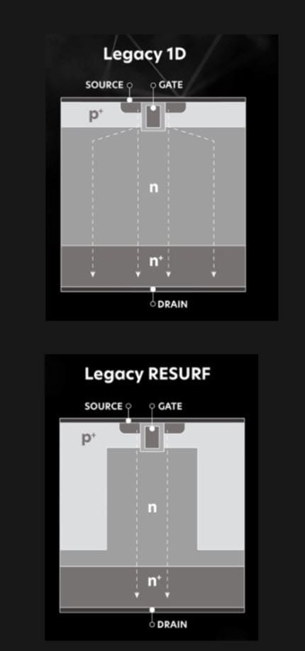
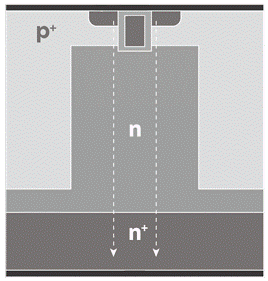
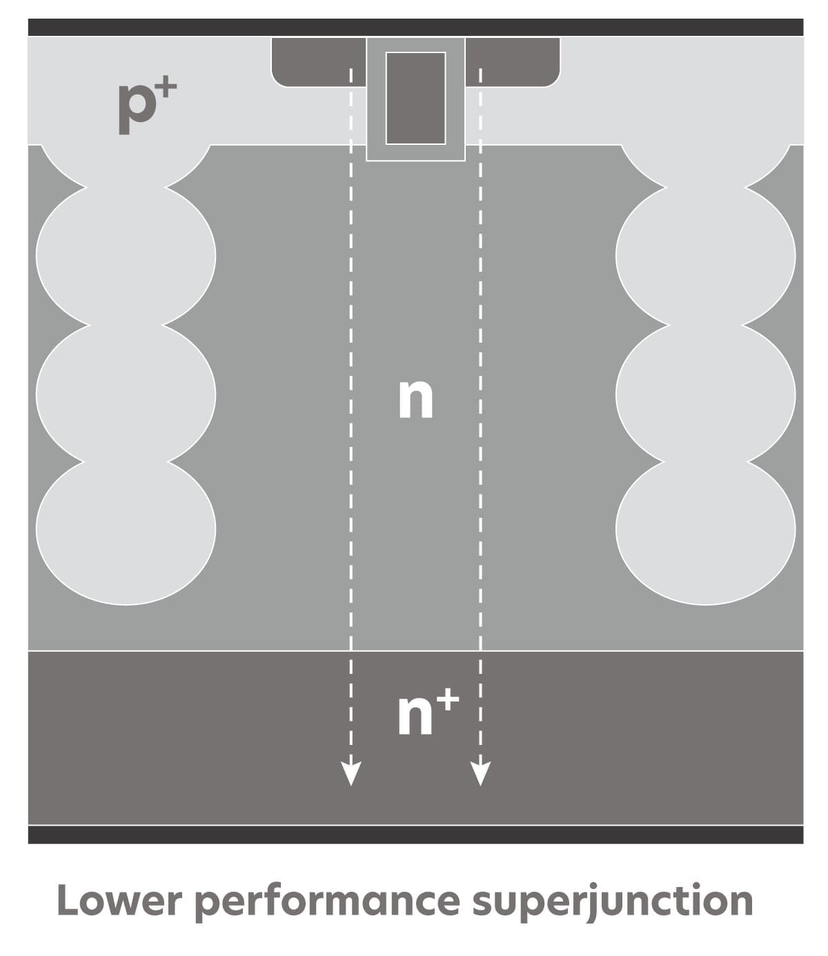
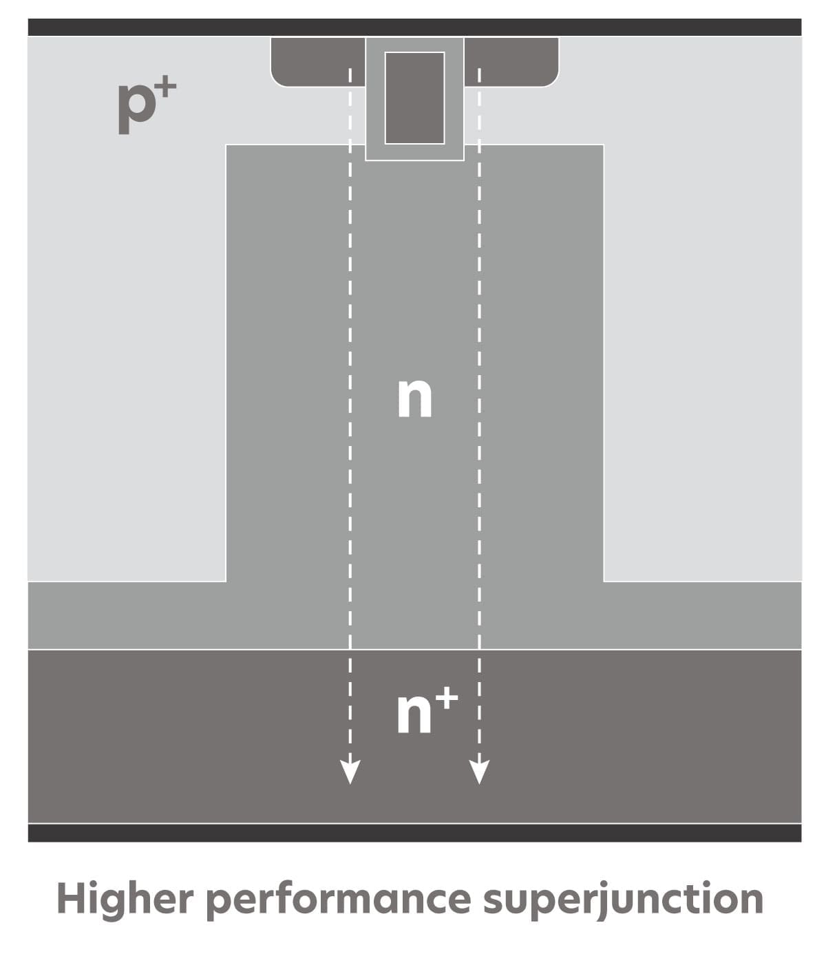
The Legacy 1D MOSFET (left) and RESURF/Superjunction (right). By using alternating n- and p-type columns in the drift region the Superjunction structure reduced RDS(on) without reducing the breakdown voltage but also halved the conduction area
Planar 1D MOSFETs “HEXFET”
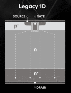 The planar 1D MOSFET, often exemplified by International Rectifier's (IR) HEXFET™ technology, marked a significant advancement in silicon power semiconductors during the late 1970s and 1980s. Introduced by IR in 1979, the HEXFET was one of the first commercially successful power MOSFETs, featuring a unique hexagonal cell structure that optimized gate density and reduced RDS(on) compared to earlier bipolar transistors. This design allowed for faster switching speeds, lower drive power requirements, and improved efficiency, making it ideal for applications like motor controls, power supplies, and automotive electronics.
At its core, the planar 1D MOSFET uses a vertical structure where the drift region is uniformly doped, and the gate is formed on the surface in a planar configuration. This allows 100% of the drift region to be dedicated to conduction, maximizing current-carrying capability without the need for compensating structures. The HEXFET's hexagonal geometry further enhanced this by enabling tighter cell packing, which lowered RDS(on) while maintaining high breakdown voltages (BV).
Over time, the technology evolved with key improvements, such as the introduction of trench gate architectures in the 1990s. Trench gates, where the gate electrode is etched into a vertical trench, created a vertical channel that further reduced RDS(on) by shortening the channel length and improving electron mobility. This enhancement built on the planar foundation, allowing for even better performance in medium-voltage applications.
However, the planar 1D MOSFET has inherent limitations tied to silicon's material properties. In these devices, the specific on-resistance (Rsp) increases with the breakdown voltage raised to the power of approximately 2.5 (Rsp ∝ BV2.5), following the theoretical silicon limit for unipolar devices. This relationship arises because higher BV requires a thicker, lower-doped drift region to support the voltage, which in turn increases resistance.
As a result, planar 1D structures like the HEXFET were most effective for low-voltage applications (typically below 200 V) where RDS(on) can remain competitively low. For higher voltages, the resistance becomes prohibitively high, leading to increased power losses and reduced efficiency, which prompted the development of more advanced architectures like Superjunction MOSFETs.
RESURF Superjunction MOSFETs for >400 V
Building on the limitations of planar 1D MOSFETs, the RESURF (Reduced Surface Field) Superjunction MOSFET emerged as a transformative technology for high-voltage applications above 400 V. Patented in the early 1980s and commercialized by 1998, Superjunction devices employ a two-dimensional (2D) structure with alternating vertical p-type and n-type columns in the drift region. This design leverages charge compensation to achieve superior performance, allowing for higher doping levels in the n-columns to minimize RDS(on) while preserving high breakdown voltage.
The key innovation lies in how the p-type columns reshape the electric field during off-state operation. In traditional planar devices, the electric field peaks sharply at the surface, forming a triangular profile that limits BV and necessitates thicker, lower-doped drift layers for higher voltages. Superjunction's p-n junctions enable lateral depletion: as reverse bias is applied, the p-columns deplete the adjacent n-columns sideways, creating a more uniform, rectangular electric field distribution across the drift region. This flattening reduces peak field intensity, supports voltage blocking of 13-15 V/µm, and allows the device to handle higher BV without proportionally increasing resistance.
As a result, Superjunction MOSFETs break the silicon limit of planar structures, where Rsp scales with BV raised to the power of approximately 2.5 (Rsp ∝ BV2.5). Instead, Rsp increases linearly with BV (Rsp ∝ BV), dramatically lowering losses in high-voltage scenarios like power supplies, EV chargers, and industrial drives. Today's advanced Superjunction devices achieve RDS(on) as low as 7 mΩ for 600 V.
Field Plate Technology for 300 V and Below
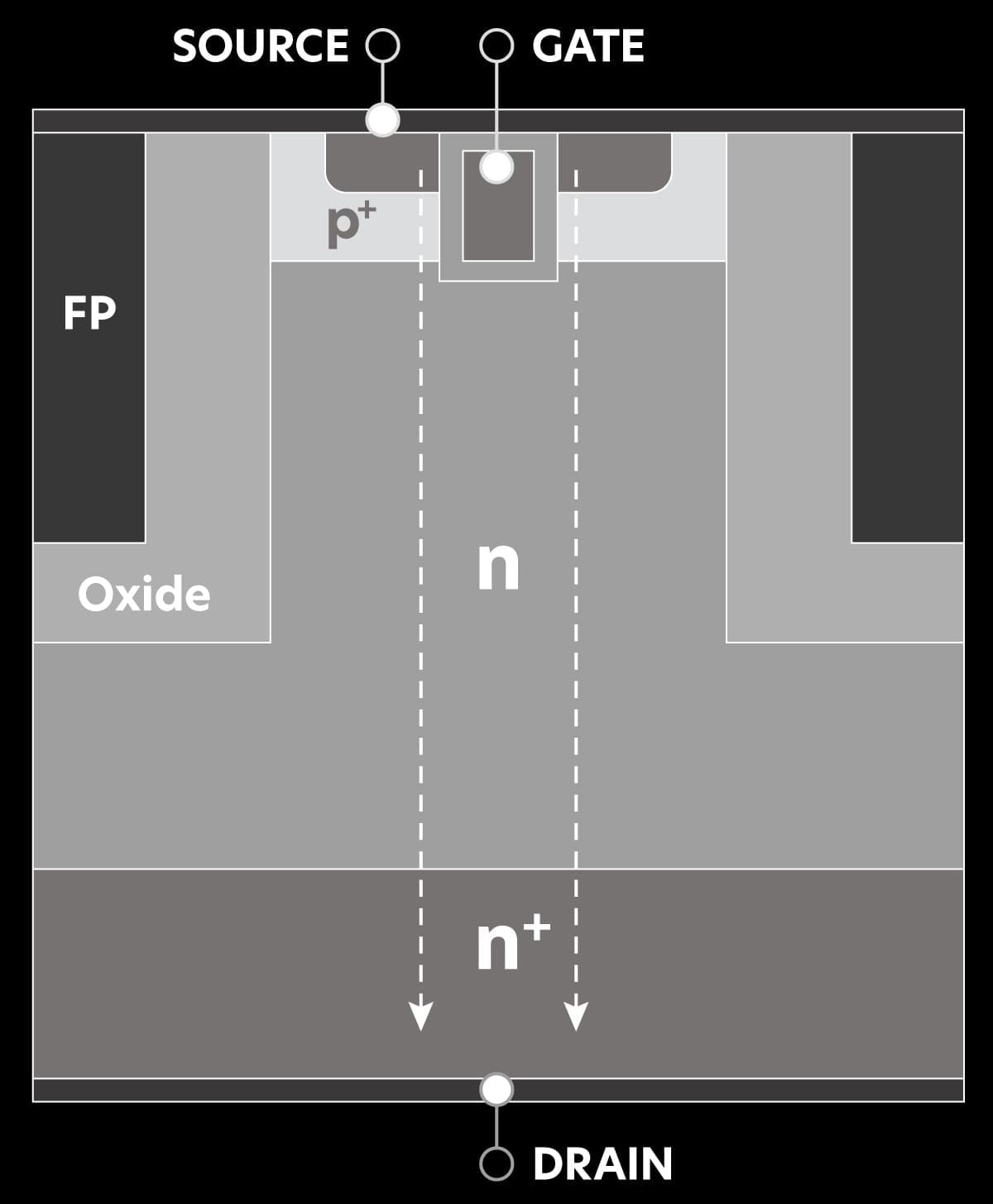
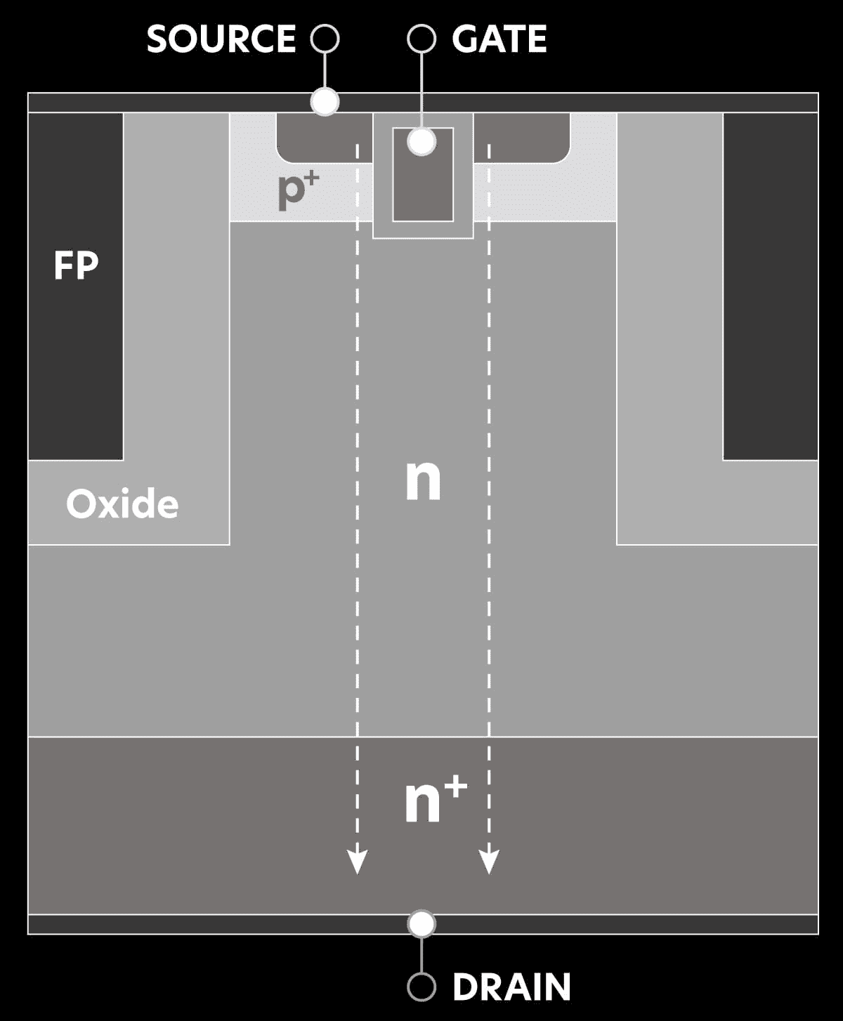 Field plate technology has become a cornerstone for silicon power MOSFETs in medium- to low-voltage applications, particularly below 300 V, where Superjunction structures face challenges in achieving narrow p-type columns. This approach utilizes trench-based designs with polysilicon electrodes, insulated by thick oxide layers, embedded within the drift region. These field plates act as electrostatic shields, reshaping the electric field to create a uniform distribution through capacitive coupling, akin to the RESURF effect seen in Superjunctions, but without relying on p-n junctions for charge balance.
In the off-state, field plates laterally deplete the n-type drift region (mesa), enabling higher doping levels in the conduction path while maintaining BV. This reduces specific Rsp, with Rsp scaling approximately with BV1.5-2, offering a significant improvement over planar 1D MOSFETs. The advanced "split-gate" configuration, where the gate and field plate are separated within the trench, further optimizes performance by minimizing gate-drain capacitance (Cgd), enhancing switching efficiency. State-of-the-art processes achieve mesa widths as low as 0.5 μm, yielding silicon efficiencies around 40% and RDS(on) values below 5 mΩ for 100 V devices, making field plates highly effective for applications like DC-DC converters and battery management systems.
Future roadmaps focus on tightening mesa widths and increasing epitaxial doping to further reduce Rsp, maintaining field plate viability for low-voltage, high-efficiency applications. However, scaling challenges and performance trade-offs at higher voltages set the stage for alternative technologies to address broader voltage ranges.
Limitations of Superjunction and Field Plate Technologies
Superjunction MOSFETs, while revolutionary for high-voltage applications, face significant manufacturing challenges that limit scalability and cost-effectiveness. Traditional fabrication relies on multi-epitaxial (multi-epi) growth, where the drift region is built layer by layer – typically 5-10 μm thick in lower-performance devices – requiring doping of alternating p- and n-type regions after each epi growth.
For a 55 μm stack supporting 600-650 V, this can necessitate 5-11 layers, resulting in wavy p-pillars due to diffusion and misalignment, as seen in cross-sections of coarser processes. Higher-performance variants employ finer epi steps (around 2-3 μm), enabling tighter charge balance and lower RDS(on), but demand even more layers (up to 20+), additional mask steps, and stringent process control to minimize defects and maintain uniformity. These complexities increase fabrication costs, cycle times, and yield risks, constraining further density improvements without exponential rises in complexity.
Field plate technologies, effective for voltages below 300 V, encounter limitations as BV increases due to oxide thickness (tox) requirements. Field plates are tied to source so oxides must be included to block voltage in the structure. Tox scales proportionally with voltage to withstand electric fields, widening trenches and reducing silicon efficiency: from ~39% at 100 V (tox ≈600 Å) to ~9% at 300 V (tox ≈1500 Å). This forces larger cell pitches (e.g., from 2.55 μm to 4.2 μm between 100 V and 150 V), compromising RDS(on) and scalability, especially above 100 V where manufacturing thick, uniform oxides becomes impractical.
Faced with these barriers in silicon-based architectures, and without ideas or invention for where to go next in silicon, the industry turned to wide bandgap semiconductors like SiC and GaN for breakthroughs in efficiency and power density, as customer demands for higher performance outpaced incremental silicon advancements.
Faced with these barriers in silicon-based architectures, and without ideas or invention for where to go next in silicon, the industry turned to wide bandgap semiconductors like SiC and GaN for breakthroughs in efficiency and power density, as customer demands for higher performance outpaced incremental silicon advancements.
Benefits of Silicon
Despite the challenges, silicon remains a crucial material in power electronics due to its inherent advantages:
Supply Chain
Silicon has a well-established and mature supply chain. Silicon is abundant and therefore low-cost. The infrastructure for manufacturing silicon devices is also extensive and, with foundries located across the world, is a secure supply chain.
This ensures a reliable and stable supply of silicon power devices. Supply chain stability in GaN and SiC is still maturing and can present challenges for some applications.
Cost
Silicon power devices are significantly less expensive than WBG devices. The mature manufacturing processes and high production volumes contribute to the lower cost of silicon devices. Total cost of ownership, including device cost, system-level costs, and long-term reliability, often favors silicon in many applications.
The cost of switching to GaN or SiC can be substantial, involving not only the higher device cost but also the cost of redesigning power electronic systems to accommodate the different characteristics of WBG devices. Complicated gate drive requirements, parasitic inductance limitations and electromagnetic interference are just a few challenges that must be overcome.
Market Share
Silicon remains the most commonly used substrate for power semiconductors.
In 2023, Grand View Research stated silicon’s market share in power electronics (by revenue) was 88.9%. It also cited that demand was increasing.
While few reports exist showing the share based on units shipped, the significantly lower cost than either SiC or GaN suggests silicon’s market share is considerably over 90%.
SuperQ Technology
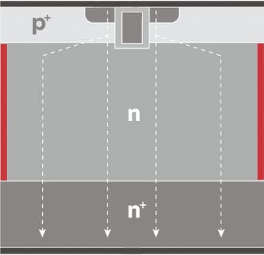
SuperQ® technology marks a transformative leap in discrete silicon power design. It was announced in 2023 and released to production in 2025 to address the limitations of traditional architectures like Superjunction and field plates. This revolutionary approach employs an asymmetrical RESURF structure, achieving near-ideal charge balance with a thinner epitaxy layer. By optimizing the drift region’s n-type conduction area – with a roadmap to nearly doubling it compared to Superjunction devices – SuperQ significantly lowers on-resistance while maintaining high breakdown voltage. This results in industry leading resistance and switching losses.
Unlike Superjunction’s multi-epitaxial complexity or field plate’s oxide thickness constraints, SuperQ leverages a simplified process with wider n-type mesas (e.g., 75% silicon efficiency vs. 50% in Superjunction) and minimal trench requirements, avoiding thick oxide dependencies. This preserves silicon’s cost-effectiveness, availability, and reliability, aligning with the established manufacturing ecosystem. The technology’s scalability across 60 V to 1,200 V ranges positions it as a higher performance alternative to existing silicon while preserving the Cost x Performance ratio that design engineers have come to expect.
Conclusion
The evolution of silicon power devices, from early transistors in the 1950s to the groundbreaking SuperQ® technology launched in 2025, underscores silicon's enduring dominance in electronics. Power MOSFETs and IGBTs have powered transformative applications – renewable energy, electric vehicles, and AI data centers – due to silicon's abundance, cost-effectiveness, and mature manufacturing ecosystem, which still commands over 90% of the semiconductor market. Milestones like the HEXFET, Superjunction, and field plate innovations have progressively enhanced efficiency and voltage handling, yet each reached inherent limits: Superjunction’s multi-epitaxial complexity and field plate’s oxide thickness constraints hindered scalability.

SuperQ emerges as a pivotal advancement, doubling conduction area, slashing on-resistance, and cutting inverter losses by up to 46%, all while preserving silicon’s economic and reliability advantages. This innovation reinvigorates silicon’s competitiveness against wide bandgap materials like SiC and GaN, which, despite their promise, face immature supply chains and higher costs. By leveraging a simplified, high-efficiency architecture scalable from 60 V to 1200 V, SuperQ not only meets escalating performance demands but also reinforces silicon’s role as the industry standard. As technology advances, SuperQ ensures silicon remains at the forefront of power electronics, driving innovation without disrupting established infrastructure.
Start Designing With SuperQ
Work with our applications engineers to assess SuperQ performance in your system and identify the best device for your design.