The whole electronics industry is built upon a pursuit of higher performance, higher efficiency, smaller size and lower cost. For years, the semiconductor sector has developed techniques, technologies and solutions in a bid to continue to meet these goals. As applications have grown more challenging, continued innovation has sought to ensure that semiconductor switches were able to keep pace with user requirements.
During the 1950s, bipolar junction transistors (BJTs) replaced vacuum tubes as the primary switching device. Later, new power semiconductors such as power diodes and thyristors were developed. These devices gradually gave way to field effect transistors (FETs) such as planar MOSFETs, heralding a significant drop in conduction losses.
While the array of power semiconductors available may seem complex, they perform just one of two tasks – blocking voltage when in the off-state and passing current with as few losses as possible in the on-state. Simple, but incredibly important to all modern power electronics.
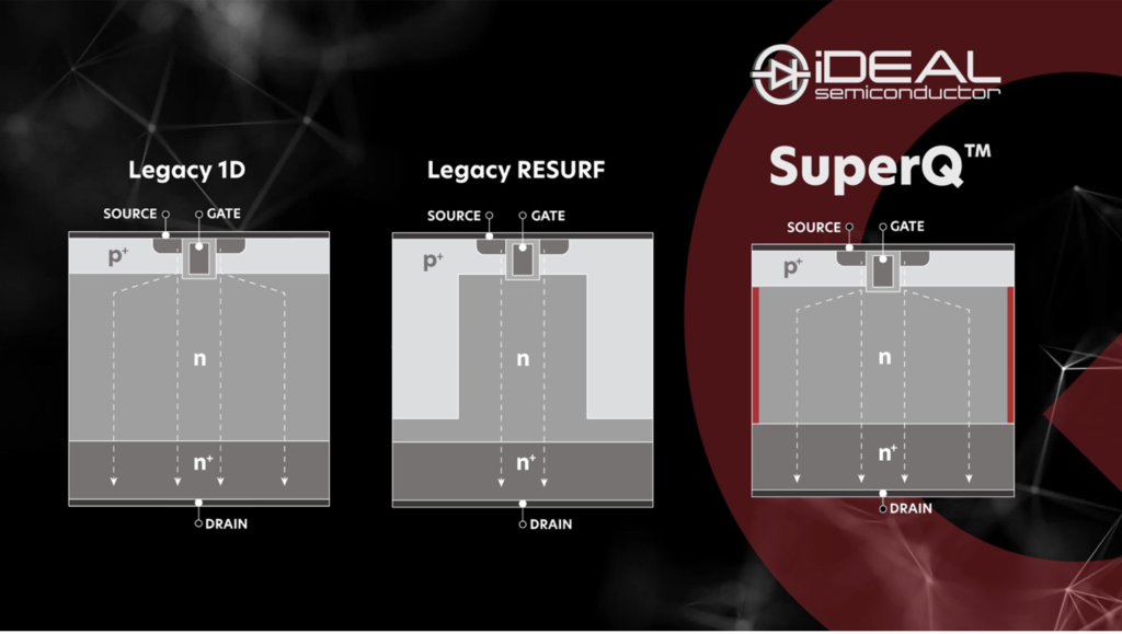
Early FET devices were known as ‘Legacy 1D’ – a reference to their one-dimensional structure. International Rectifier launched this technology under their HexFET brand in the late 1970s, primarily to improve the conduction performance offered by BJTs. With 100% of the silicon dedicated to conduction, they performed well in this regard.
However, with this type of construction, as the blocking voltage increased, the resistance increased by the square of this figure, significantly hampering conduction. Consequently, HexFET devices were only ever useful in low voltage applications or in some higher voltage, low power applications where high resistance was not an issue.
So-called ‘SuperJunction’ devices were released in the 1990s, primarily to address the blocking voltage issue using a reduced surface field (RESURF) approach. By reshaping the electric field, these two-dimensional (2D) devices ensured that the resistance rose linearly with blocking voltage – reducing the losses in high voltage HexFET devices. Typically, these 2D devices provide voltage blocking at around 13-15 V/µm.
SuperJunction devices are symmetrical structures, where the P-region and N-region are equal sizes so that charge is balanced. However, as the P-region does not contribute to conduction, the silicon utilization for conduction is only 50% (only the N-region conducts).
While many see the next step as being a change to alternate materials, such as WBG, this is not the case. In fact, the future of power semiconductor devices lies not in the choice of material, but in the use of advantageous structures, such as SuperQ™ which will improve the performance all materials, including silicon, SiC and GaN.
Delivering conduction performance which many believed was not possible with silicon, SuperQ is an asymmetrical structure that is designed to maximize the N-conduction regions, ensuring that up to 95% of the structure is dedicated to low-loss conduction. This innovative approach gives a thinner Epi with higher doping, creating a significant performance advantage. It also improves voltage blocking compared to SuperJunction, achieving 19-20 V/µm.